
X-ray microanalysis, EDX and imaging by means of Scanning electron microscopy, SEM
There are various fields of application for scanning electron microscopes in combination with energy-dispersive X-Ray microanalysis, EDX. Below you find some exemplary applications.
Many more issues can be clarified by means of our microstructural and microanalytical test procedures.
Our services for you:
- X-ray microanalysis, EDX
- Element mappings, linescans
- Imaging by means of SEM
- Grain size determination, fibre length
- Damage assessment
If you have any questions, please do not hesitate to call us.

Details concerning the listed areas of application:

The energy-dispersive X-ray microanalysis, EDX using scanning electron microscope
The energy-dispersive microanalysis, EDX using scanning electron microscope is used for the qualitative and quantitative analysis of minimal sample volumes down to µm3-size like
- Inclusions
- Contaminations
- Individual dust particles
- Efflorescences like so-called out-bloomings
and for
- Chemical characterizations of unknown materials
Some applications:
 |
 |
 |
 |
|
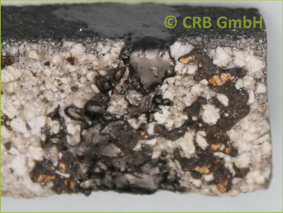
metallic inclusions in slag |
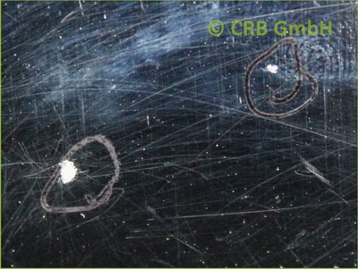
inclusions in steel sheets |
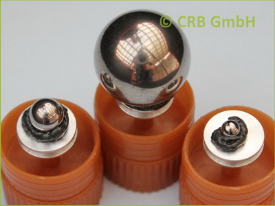
balls from a bearing |
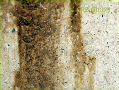
discolorations on ceramics |
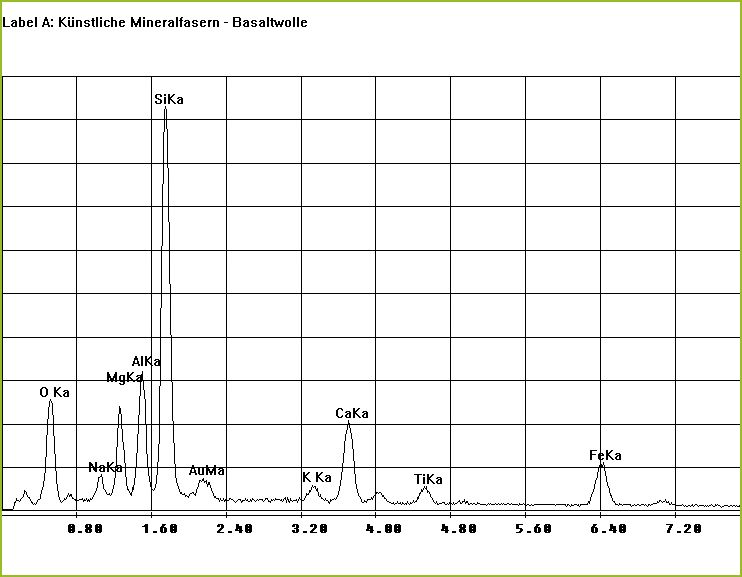
Elemental analysis, qualitative |
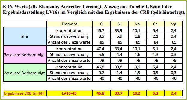
Elemental analysis, semi-quantitative to quantitative |
 |
 |
|
The qualitative X-ray microanalysis is carried by means of energy-dispersive element spectra. |
Ideally, semiquantitative to quantitative X-ray micro analyses are carried out using samples with a plane and flat surface. The example on the right shows the results of a collaborative study microanalysis. |

Element mappings and linescans
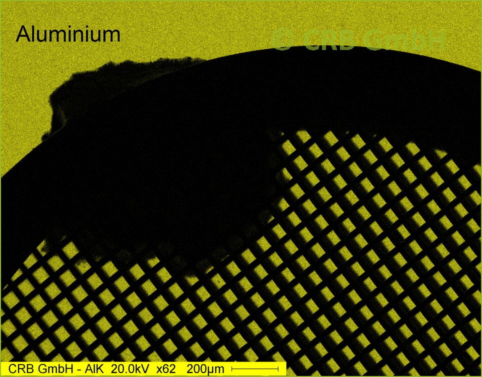
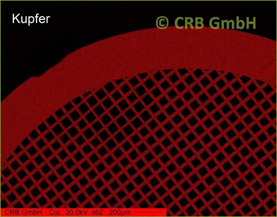
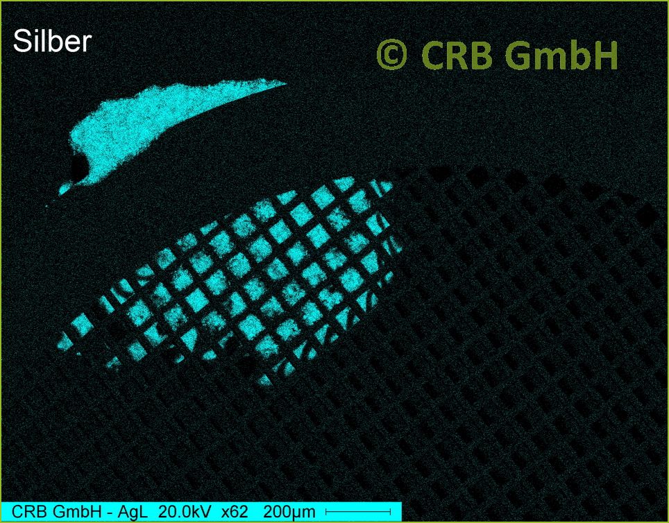
The Scanning Electron Microscope, SEM in combination with an energy-dispersive detector system, EDX is perfectly suited for the presentation of material contrasts, element distributions, by element mappings and linescans.
Ideally, mappings and linescans are carried out using samples with a plane and flat surface:
Metallic workpieces or polished grindings of oxidic raw materials are particularly suitable.
EDX - Linescans
 |
 |
|
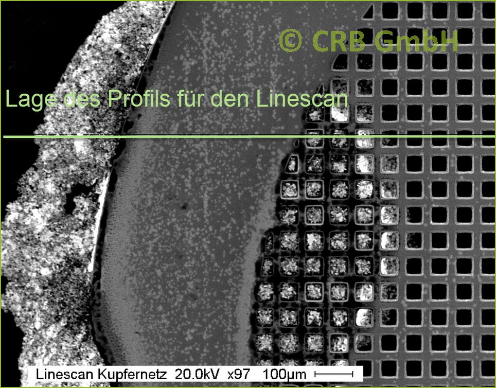
SEM image of a copper net glued on an aluminium plate with silver coating. The position of the profile is highlighted in green. |
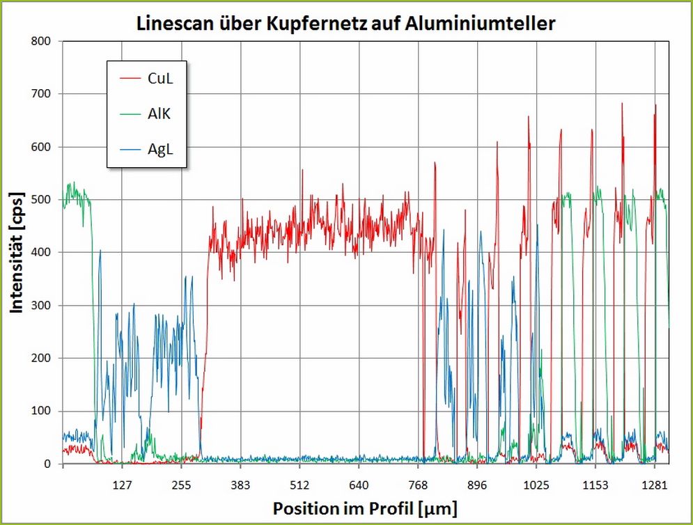
EDX linescan for the elements aluminium (green), copper (red), silver (blue) along the limit line in the above diagram. |
EDX element mappings
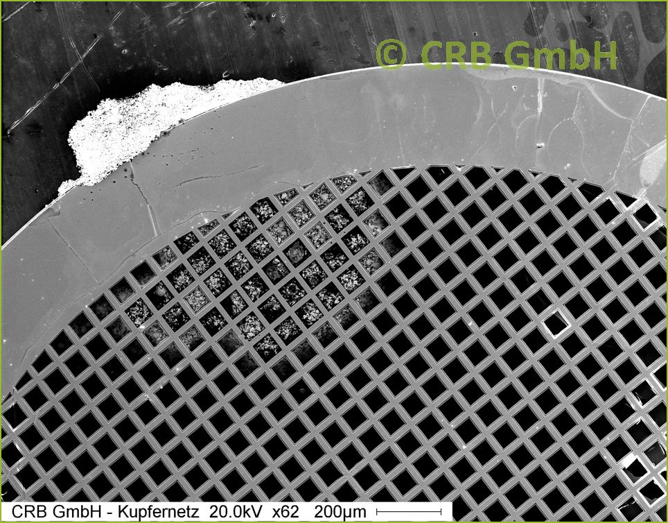 |
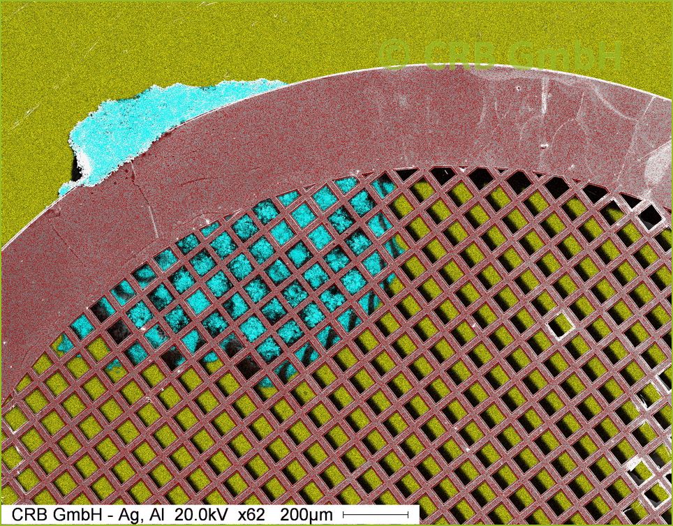
SEM image of a copper net glued on an aluminium plate with silver coating. Image width approx. 1,3 cm. |
|
|
|
 |
 |
|
Element mapping for aluminium |
Element mapping for copper |
 |
 |
| Element mapping for silver |
Combined element mapping for the elements aluminium, copper, silver overlapped by SEM image. |

The formation of SEM images
|
Being a high – resolution image formation device the Scanning Electron Microscope can ideally be used for imaging ? surfaces and microscopic structures. The abundance of options for its use in natural sciences, technical and medical applications make it impossible to offer a complete list right here. This method allows images with different resolutions and in TIF format without losses or as JPEG file. We offer the following image resolutions:
|
 |
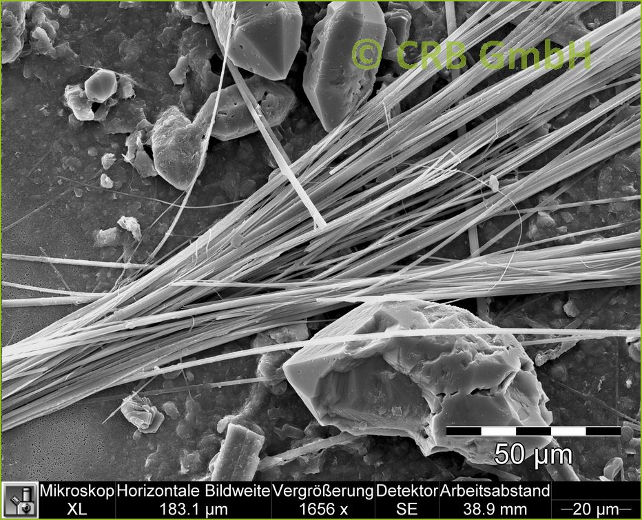 |
SEM images of amphibole, amosite, next to idiomorphic quartz crystals, Approx. 1600X magnification , Image width approx. 190 µm |
|
|
|
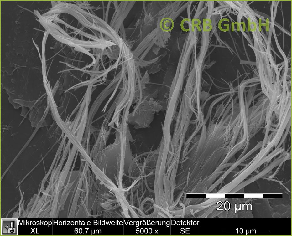 |
SEM images of chrysotile asbestos in bituminous glue, Approx. 5000X magnification, Image width approx. 60 µm |

Grain size distribution, determination of fibre diameter
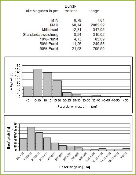
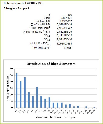
WWherever classic procedures like laser granulometry and sieve analysis cannot be applied/ are not suitable geometric features like grain size and fibre diameter distribution or e.g. the Lenth-Weighted Geometric Mean Diameter, LWGMD, of man-made mineral fibres by means of SEM can be determined
- qualitatively using imaging
- quantitatively by determination of particles and fibres
If you have any questions do not hesitate to contact us.
 |
 |
|
Determination of fibre diameters and fibre length by means of SEM |
Determination of the Lenth-Weighted Geometric Mean Diameter, LWGMD, of man-made mineral fibres. |

